LT6502b progress
A lot has happened with LT6502b since my last post.
Firstly the WiFi modem is now working, I finished the UART in a CPLD and it works a treat 🙂
Secondly it’s now running at 10MHz, I can’t seem to get much above that, yet.
Thirdly I’ve now added the nanoSwinSID chip onto the PCB and fitted the remaining keys.
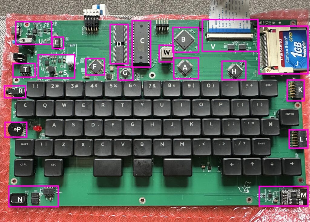
- A – WDC65C02 CPU, the heart of the laptop
- B – ATF1508 CPLD, this is the glue logic and address decoding for everything, it has the WIFI UART in, Clock stretching and a whole bunch of other essentials
- C – SST39SF010 ROM, technically a flash ROM, this holds the “bios” or operating system, it holds EhBasic and Wozmon
- D – RAM, 48K of RAM, of which the lowest 2K is for the OS to use for input buffers, load/save buffer, stack, etc.
- E – FT245, USB Serial chip, this is our console and is mirrored with the display and keyboard
- F – ATMEGA644, Keyscan chip, it scans the keys and sends data over serial to the CPLD, it also talks to the WiFi over serial and provides a buffer between the WiFi modem and CPLD which has no serial buffer.
- G – NanoSwinSID, an ATMEGA88 overclocked running SID emulation. I’m aware these aren’t the most accurate emulations, but that’s not what I was after, I just wanted something simple to integrate that would give me more sound options than just “beep”.
- H – WDC65C22, VIA chip, giving us a timer and two 8 bit I/O ports
- J – Compact flash, not DOS compatible but can store 1024 programs, each up to 64KByte. Not a huge amount, but more than enough for my needs.
- K/L – 8bit IO ports, arranged like PMODs but at 5V, these could easily be used as Joystick ports.
- M – ESP01 WiFi Modem, very simple little thing, uses the AT command set and communicates via Serial
- N – Speaker and amplifier for beeps and SID.
- P – Volume control for built in speaker
- R – line output for sound
- S – Battery charging circuit
- T – Reset Circuit
- U – Power circuit for USBC-PD
- V – Display interface and level shifters (3.3V switch mode PSU at top right of PCB).
- W – Main clock (currently 20MHz), double that of the CPU speed, in a socket for ease of change.
There are still a couple of things to sort;
- The SID output is incredibly quiet, much quieter than it should be.
- “Shift” on the keyboard doesn’t yet work
- The case needs finishing, I’ve held off until I was sure that I wouldn’t need drastic changes to the PCB
- I would like to try and get to 14MHz (rated speed of the 65C02), I believe the ROM is making it difficult to go beyond 10MHz.
But I’m very happy with the progress. In regards the ModWires, one of these is no longer needed and the other was needed to signal to the CPLD when data is waiting to be sent from the KeyController/WiFi Modem, I’ve updated the Schematics and PCB layout in the repository.